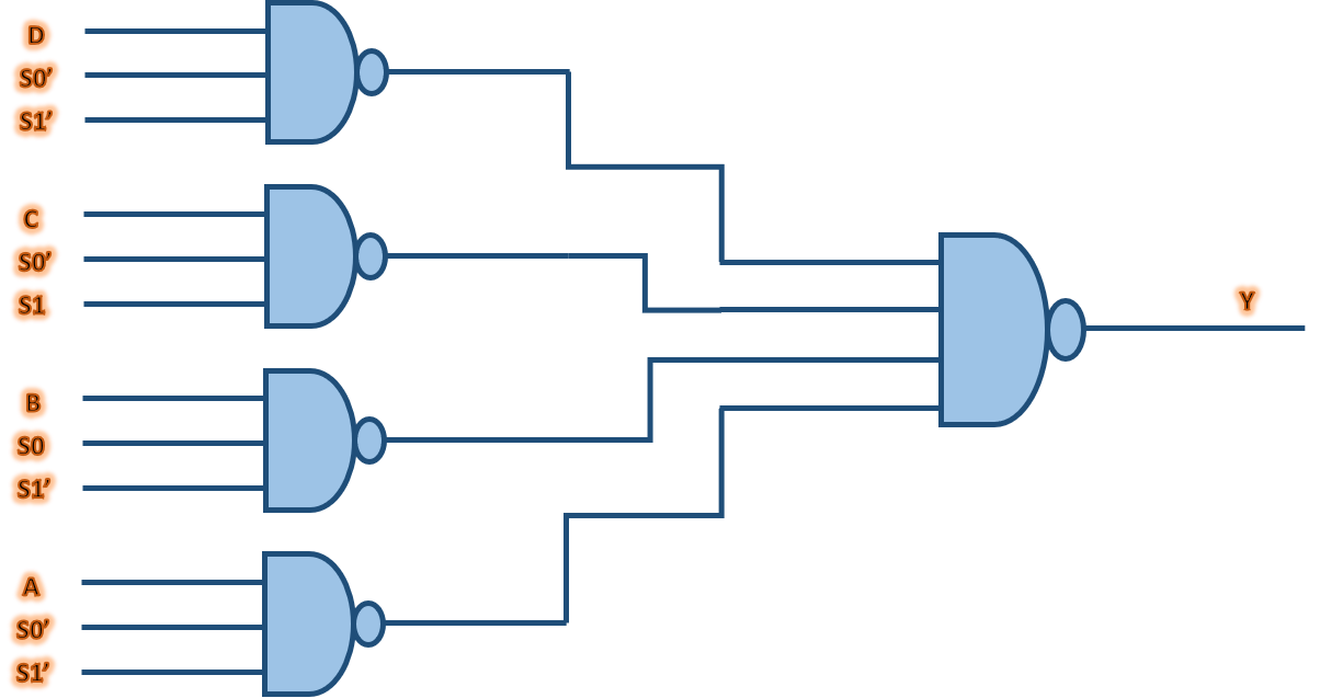
Mux multiplexer graphical circuit Mux multiplexer verilog 2x1 code technobyte 4 to 1 multiplexer circuit diagram and truth table
VLSI n EDA
Multiplexer mux circuit electronics gates nand inputs select boolean multiplexing combination given Mux constructed digital The multiplexer (mux) and multiplexing tutorial
Mux 8x1 wiring schemas 2x1
8x1 mux logic diagram : 8x1 mux logic diagramMux nand 4x1 using gates implement implementation vlsi eda figure below Vlsi n edaVerilog code for 2:1 multiplexer (mux).
Virtual lab .


4 To 1 Multiplexer Circuit Diagram And Truth Table - Wiring Diagram

VIRTUAL LAB - ECE18R369 DIGITAL VLSI DESIGN

The Multiplexer (MUX) and Multiplexing Tutorial
VLSI n EDA

8X1 Mux Logic Diagram : 8x1 Mux Logic Diagram - Wiring Diagram Schemas
